
Time:2024-10-30 Browse: 150
I. What is ESD?
ESD, which stands for electrostatic discharge, occurs when many materials that can conduct electricity accumulate charges. This can happen due to triboelectrification (friction between materials) or electrostatic induction. In such instances, an object forms a fixed charge (static electricity) on its surface. When this object is placed in close proximity to another charged object or material, a voltage difference causes a current to flow between them until charge balance is restored.
Consequently, electrostatic discharge can be defined as the instantaneous current flow between two charged materials or objects caused by contact, short circuit, or dielectric breakdown.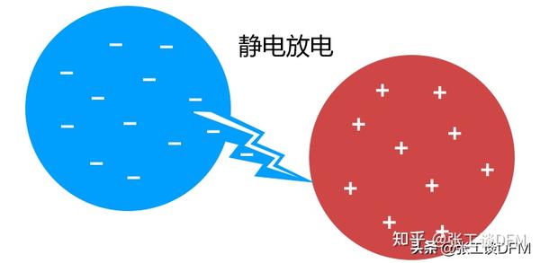
For consumer products, ESD and dielectric breakdown in air typically occur when the electric field between two points exceeds 40 kV/cm. Factors such as air pressure, temperature, and humidity can influence the electric field strength. For example, high humidity in certain environments can make the air more conductive, dissipating some charges and increasing the voltage required for ESD.
II. How does ESD affect PCBs?
Static electricity is relatively common in daily life. However, the voltage of static charge can reach several thousand volts, which can cause significant harm to components.
When this voltage difference is sufficiently large, a conduction path for current emerges, resulting in a massive current pulse. As the current pulse develops, high heat dissipates within the components and conductors of the PCB itself. Under extreme field strengths and generated currents, the PCB may be damaged and components may be destroyed.
This heat dissipation is essentially an IR voltage drop, where the natural DC resistance of the components in the PCB generates a voltage drop and reaches a high temperature. ESD can occur in some common locations on the PCB. Therefore, ESD protection in the PCB should focus on specific areas. For example:
Connectors themselves are not an ESD source. However, the static charge accumulated on them can lead to ESD. Actions such as inserting a chip, unplugging a cable, or pressing a button can pose electrostatic risks to the device. Due to the transfer of static charge on floating conductors, floating pins may generate ESD. Finally, when a connector is inserted into a socket, ESD may occur, resulting in a spark.
The metal shield and floating pins on connectors are common locations for ESD events in some consumer and industrial products.
A simple solution for handling floating pins is to ground them. Shielded connectors should also have a grounded shield layer connected to the chassis and ultimately to the ground. It should be a low-impedance connection directly connected to the chassis, not provided through a capacitor or by routing ESD current to ground through the PCB.
Almost every element of PCB design, including traces, routing, layers, component placement, and spacing, can affect PCB ESD protection. Therefore, ESD protection circuits must be considered early in the design process.
III. ESD protection circuit design
TVS diode protection circuits are one of the most common in non-industrial low-voltage settings. Compared to other ESD protection elements embedded in power management ICs or microcontrollers, TVS surge diode protectors can provide higher voltage suppression, as shown in the following example.
The following figure shows an example of an ESD protection circuit consisting of parallel TVS diodes on differential I/O.

Under normal circumstances, diodes D1 and D2 are reverse biased. As long as the input voltage is greater than the power rail voltage, diode D1 will become forward biased and conduct. Similarly, when the input voltage is lower than ground, diode D2 becomes forward biased and conducts from ground to the input.
The following figure shows a zener diode used in an ESD protection circuit on a single-ended buffer I/O.
The above circuit can utilize some simple diodes with high reverse bias breakdown voltage (such as zener diodes), or TVS diodes combined in parallel or back-to-back configurations. The main factors for determining which type of diode to use are breakdown voltage and forward current.
TVS diodes are divided into two types. Both types act as open circuits under normal operating conditions and as short circuits to ground when an ESD surge occurs.
The following figure shows a unidirectional TVS suppression diode on the power rail of a protected component.
The way a unidirectional TVS diode protects a circuit from ESD is by blocking or allowing ESD current to flow depending on its polarity.
During the positive cycle of transient ESD, one of the two diodes is forward biased and the other is reverse biased. This means that one diode conducts due to its forward bias while the other diode operates in avalanche mode. In this way, both diodes form a path from the ESD source to ground. During the negative ESD cycle, the diodes exchange their modes, creating a path again and keeping the circuit protected.
This circuit is designed specifically for overvoltage on telecommunication lines. Compared to TVS diode arrays, TISP4 provides a certain degree of general protection against ESD events and overvoltage events from other sources.
The selection of protection devices depends on many factors. Different models and types are designed for different voltage ranges, operating voltages, event durations, response times, and so on.
3. Other ESD suppressor components
In addition to the above, there are several other ESD suppressor components, such as multilayer varistors, gas discharge tubes, and polymer-based suppressors. ESD suppression components are used to reduce the ESD voltage below a specific limit to protect a circuit or group of components.
The suppressor component or circuit is connected in parallel to the vulnerable line, keeping the low ESD voltage within a certain limit and shunting the main ESD current to ground. Generally, relevant circuit examples can be found on the datasheet.
4. Specific case: Gas discharge tube + TVS diode
One strategy for handling high voltages is to use a gas discharge tube in parallel with a TVS diode and an inductor. The inductor and TVS diode act like a low-pass RL circuit, providing additional filtering and slowing down the rise time of the ESD pulse.
The following circuit is basically a low-pass filter with a large time constant. Therefore, this circuit will allow the nominal DC voltage to pass while providing high impedance to the ESD current passing through the discharge tube. The fuse at the input provides additional protection against large ESD voltages.
The following figure shows the ESD protection circuit design using TVS diodes and gas discharge tubes.
IV. ESD protection in PCB layout
All PCB components and traces have parasitic inductance. In a typical protection scheme, there are four: the inductance between the ESD source and the TVS array (L1 and L2), the inductance between the TVS and ground (L3), and the inductance between the TVS and the protected integrated circuit.
Only when L4 is greater than L1 - 3 can the ESD current be forced to ground.
The following figure shows the PCB layout of a project. As can be seen from the figure, this part of the PCB has a USB port. To protect the FT231X UART (U1), we placed a USBLC6 - 4SC6 ESD suppressor (U2) on the path between it and the port.

There are two points to note here:
ESD generates strong voltage pulses that can cause electromagnetic interference (EMI) to other nearby signal lines. The main source of radiation is located between the ESD source and the suppressor that acts as an antenna.
If possible, in the design, the suppressor area should be kept away from other circuits and unprotected traces, otherwise they will transmit the ESD signal to other ICs. Even without considering the inductance of each line, the protected line and the adjacent unprotected line can act as capacitors, allowing voltage surges to transfer between the two lines. The following figure illustrates how an ESD pulse can couple to an unprotected line:

How ESD couples to nearby traces because these two traces act like a capacitor.
Another way to limit EMI is to use straight lines and short paths, as corners can radiate EMI. In this case, using straight lines is not possible. Instead, we used 45° bends.

The following figure shows the PCB ESD protection circuit layout.
3. Correct use of VIA
In multilayer PCBs, vias can be used as parasitic inductance to reduce unnecessary traces. In the following figure, the ESD source and the protected IC are on the same layer, while the TVS is on another layer. Here, the via acts as L2, causing the ESD current to split between the TVS and the IC. Therefore, this layout must be avoided.
In this case, although the TVS is on its path, part of the ESD current will flow to the protected IC.

The worst PCB layout.
Ideally, the ESD source and TVS should be on the same layer, as shown in the following figure. In this way, the ESD current first flows through the TVS protection pin and then through the via to the protected circuit. In this case, the TVS is directly on the path from the ESD source to the protected circuit.

The best PCB layout for ESD protection.
In this particular PCB design, the ESD source (USB connector) has two traces on two different layers. But it is impossible to place the ESD source and TVS on the same horizontal plane, so an acceptable layout is adopted.
Keep up on our always evolving product features and technology. Enter your e-mail and subscribe to our newsletter.
Address one: No. 29 Xinhe Road, Shangmu Baolai Industrial Zone, Pinghu Street, Longgang District, Shenzhen City, Guangdong Province


